

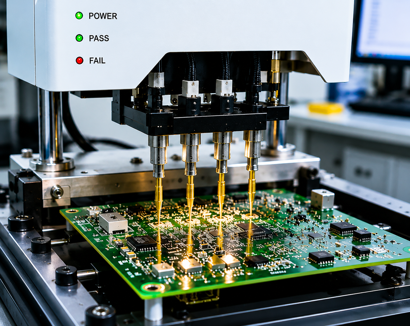
Comprehensive testing is the cornerstone of our quality assurance process. We offer a full suite of electrical, functional, and environmental testing services to ensure every PCBA performs exactly as designed — before it leaves our facility.
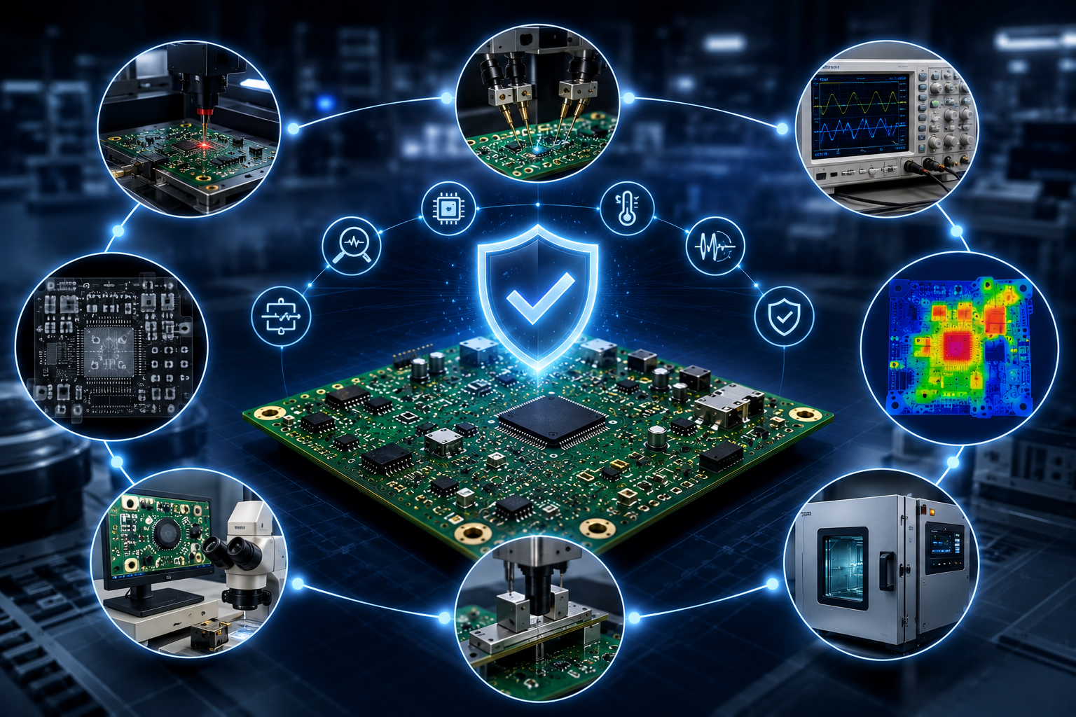
In-Circuit Testing (ICT) — bed-of-nails testing for full component verification
Flying Probe Testing — flexible, fixture-free electrical testing for prototypes and low volumes
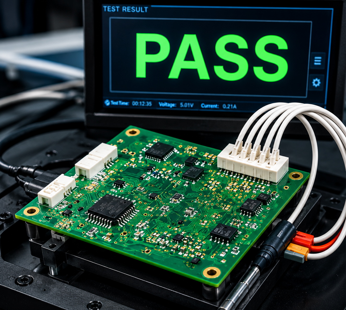
Functional Testing — powered-up verification against design specifications
Burn-In Testing — extended stress testing to screen for infant mortality failures
Automated Optical Inspection (AOI) — high-resolution camera inspection for solder and placement defects
X-Ray Inspection — internal solder joint inspection for BGAs and hidden connections
Our testing engineers work with your design documentation to develop tailored test plans that maximize coverage and minimize escape rate.
Test coverage analysis and optimization
Custom test fixture design and build
Python and LabVIEW-based functional test development
Boundary scan (JTAG) testing for complex digital boards
Environmental stress screening (ESS) — temperature cycling, vibration
Detailed failure analysis and corrective action reporting
Our rigorous testing approach delivers measurable benefits for your production quality.
Typical ICT fault coverage > 95% for populated boards
Reduce field returns with early defect detection
Catch component shortages, wrong parts, and solder defects
Batch and serial number traceability for every tested unit
Detailed test reports with pass/fail data for every board
Compliant with IPC-7711/7721 rework and repair standards
© VR Della Smart Tech-2025 | All Rights Reserved.